
“What could we do with layered structures with just the right layers?” asked Richard Feynman in his famous 1959 lecture, “There’s plenty of room at the bottom.”
ECE Professor Kaustav Banerjee, in collaboration with colleagues at Harvard University and Rice University, have provided a possible pathway toward realizing that dream, as explained in the feature story, “Two-Dimensional van der Waals Materials,” published in the September 2016 issue of Physics Today.
The featured article provides an overview of the physics, technology, and device applications of 2D materials including graphene and beyond-graphene 2D materials, as well as their wide variety of heterostructures forming completely new materials known as “van der Waals solids”. Banerjee and colleagues also discuss the prospects of employing such 2D materials for realizing layered nano- structures devices and circuits with atomic precision - a scientific dream of renowned physicist Richard Feynman.

The experimental demonstration of graphene in 2004 opened up a window to the world of 2D materials. This triggered a surge of scientific activities on various 2D crystals including single layers of insulating hexagonal-boron nitride (h-BN), several semiconducting dichalcogenides (such as MoS2 and WSe¬2), complex oxides, metals, semimetals and even superconductors, with novel electronic properties and unique physics.
Banerjee’s Nanoelectronics Research Lab has made strides in advancing the understanding of 2D materials physics. His seminal contributions include overcoming the limitations of conventional bulk materials (such as silicon and III-V semiconductors) for addressing power dissipation and other fundamental challenges in nanoscale transistors, interconnects and sensors. Learn more at nrl.ece.ucsb.edu.
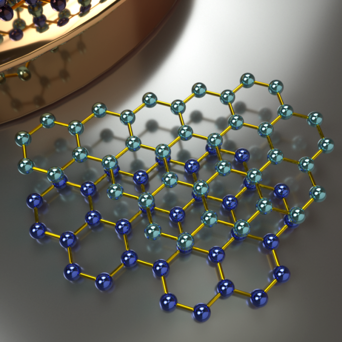
Concept art of the crystal structure (top view) of AB-stacked bilayer graphene. Credit: Peter Allen, UCSB