
In the ceaseless pursuit of energy-efficient computing, researchers in the lab of Kaustav Banerjee, professor in the Electrical and Computer Engineering (ECE) Department at UC Santa Barbara, have published a new paper in the journal Advanced Materials explaining several promising devices for processing and storing data. Arnab Pal, who recently received his PhD, is the lead author of the paper, titled “Quantum-engineered devices based on 2D materials for next-generation information processing and storage.” Banerjee says that four of the devices described in the paper — two for information processing and two for storage — are particularly promising.
One of the information-processing devices is a spin-based field-effect transistor, or spin-FET; the other is a charge-based field-effect transistor, or TFET. One of the information-storage devices is a charge-based floating-gate field-effect-transistor (FGFET); the other is a spin-based magnetic tunnel junction (MTJ). Each device is intended to address challenges associated with conventional computing in a new way.
All four devices operate at very low voltages and are characterized as being low leakage; that is, power does not drain from them when they are not on, as it does, for instance, from conventional metal-oxide semiconductor FETs (MOSFETs) in a smartphone. Because they are based on processing steps similar to those used to make MOSFETs, the devices could be produced at scale using existing industry-standard semiconductor manufacturing processes.
The most promising of the two information-processing devices, according to Banerjee, is the spin-FET, which takes advantage of the magnetic moment, or spin, of the electrons that power the device; that is, whether they are in a position of spin up or spin down relative to the electrodes for the reservoirs and drains of the carriers. While this can be done with conventional silicon materials, it is much more promising with certain ultra-thin materials, which are so thin that they are known as two-dimensional (2D) materials. In this case, the materials belong to the transition metal dichalcogenide group of compounds, which are based on transition metals.
Unlike the spin-FET, the TFET operates by taking advantage of the quantum-mechanical nature of electrons. As the result of a phenomenon known as wave-function penetration, the electrons are able to tunnel through a thin electrical barrier instead of flowing over it, as occurs in a conventional transistor. TFETs can also operate at lower voltages, thus consuming less power and generating less heat. TFETs made with 2D materials perform better thanks to their thinner and more controllable electronic tunneling barrier, which both enhances electron flow and allows the device to perform with greater precision.
In order for data to be stored securely, a device’s hard drive has to be programmed so that storage is maintained even when the power is off. To do this with a normal MOSFET, Pal says, “You have the source [electrons] and the drain [where the electrons are collected] and then the channel between them, which controls the flow of those carriers. The channel either acts as a barrier so that the electrons can’t go across — the off state — or is very conductive so that they can cross, i.e., the on state. To generate flow in a normal n-type device requires application of a positive gate bias — voltage — that attracts the negatively charged electrons from the source across the channel.
The charge-based FG-FET information-storage device works on a principle similar to that for a MOSFET, but rather than having just one gate electrode, it has two. The additional one is called a floating gate. When a MOSFET is unprogrammed, there is no additional charge on the floating gate, and, therefore, the device operates as a traditional MOSFET. However, during any programming operation, a very strong voltage is applied at the gate, causing many carriers (electrons) to be pulled from the channel and deposited there, where they become trapped. This accumulated negative gate charge makes it difficult to turn the device on, thereby programming it to be off.
But there are challenges to this method. One of them, Pal says, “is pulling a lot of charge to the floating gate, which requires a lot of power.” Further, adds Banerjee, “In order for those electrons to arrive at the floating gate to program the device, they have to tunnel through a dielectric layer. And once there, they can also leak back, creating an issue of charge retention.”
Another issue is that if many FG-FETs are placed close together — and, says Pal, “We want to put as many on the chip as possible, to, for instance, increase the capacity of a thumb drive” — the stored charges on the devices interact with each other, affecting the neighboring device. Using ultra-thin 2D materials, however, minimizes this interaction while increasing the control over the individual devices, thereby delivering high performance even when more devices are more densely concentrated on the chip.
Another approach to information storage is through the use of magnetic tunnel junctions (MTJs), which take advantage of electron spin to store data. An MTJ consists of two magnetic layers separated by a thin insulating layer, and the relative orientation of the magnetic moments of the layers determines the resistance of the device. However, similar to FG-FETs, MTJs face challenges related to power consumption, stability, and scalability. Here again, ultra-thin 2D-materials offer a potential solution by reducing interactions among neighboring MTJs, thus enabling efficient, high-density data storage.
While the devices based on 2D materials can yield improvements in terms of energy and area efficiency over those made with conventional materials, extraordinary improvements can be achieved only by changing the computing architecture. Enter the radical new architecture known as quantum computing. Based on the quantum superposition of quantum bits, called qubits, quantum computing generates parallel computations to yield massive performance gains in both speed and efficiency for select computing tasks.
The unique structural and electromagnetic properties of 2D materials that enable efficiency gains for the more-conventional charge-based qubits also make it possible to efficiently design several other newer types of qubits, called spin-, valley-, and spin-valley qubits.”
In a spin qubit, the property of the state (on/off) is defined by the electron spin, or quantum state, of the qubit, which is always either spin up or spin down. The state is changed by flipping the spin, from up to down or vice versa, to change the state of the qubit and support qubit operation.
The valley qubit operates somewhat differently, with its state being determined by the momentum of the electron, rather than its spin. The change in the electron momentum is translated to a change in the qubit state, helping to realize qubit operation.
Finally, the properties of 2D materials can also help in realizing the third type of qubit, the spin-valley qubit, the states of which are defined by both the momentum and the spin of the electrons. Because spin-valley qubits couple these two degrees of freedom, they are assumed to be more resilient to decoherence, thereby allowing longer and more complex quantum computations to be performed before quantum entanglement is lost.
In conclusion, Pal says, “The emerging devices, enabled by the unique properties of 2D materials, offer the promise of energy-efficient high-performance computing and storage, enabling beyond-Moore integration and sparking new explorations in solid-state physics and their applications.”
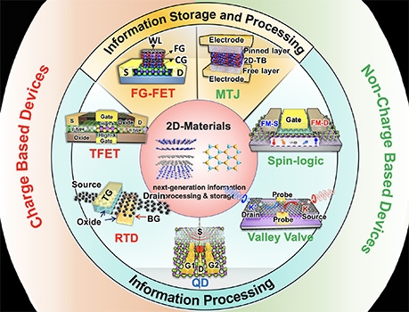
An array of charge-based and non-charge-based devices built with 2D materials may enable next-generation information processing and storage technologies. Four of the most promising devices — the spin-FET and the TFET (both for processing) as well as the FG-FET and the MTJ (both for storage) — are covered in the article. Illustration by Arnab Pal