
A key element in modern electronics, the inductor has barely changed since it was invented in 1831. A new materials approach yields a better alternative.
College of Engineering News
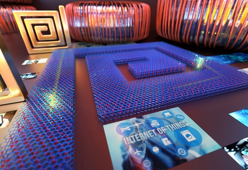
Artist's depiction of the intercalated multilayer-graphene inductor (center blue spiral), which exploits kinetic inductance to catalyze the Internet of Things. Background images show its predecessors made of conventional metal spirals (top left) or discrete coil inductors, which work solely on the principle of magnetic inductance. Illustration by Peter Allen
Feb 14, 2018
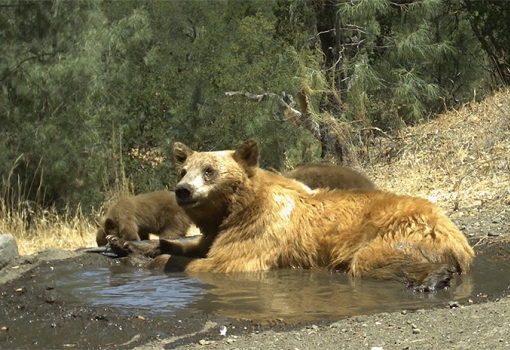
A bear with cubs at Sedgwick Reserve
Feb 13, 2018
UCSB computer scientists combine big data and machine learning to sort through millions of images and support ecological research.
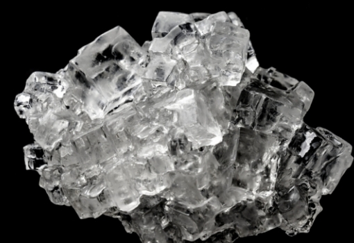
Cubic salt crystal aggragate
Jan 30, 2018
UCSB researchers unlock another piece of the crystal-growth puzzle.
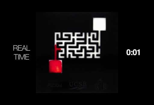
Jan 24, 2018
Fluid dynamics drive the action in a script featuring red dye, milk, and a maze of tension-induced interactions.
Photograph by Viferico - Own work, CC BY-SA 4.0, https://commons.wikimedia.org/w/index.php?curid=41177333
Jan 24, 2018
Shuji Nakamura won the 2014 Nobel Prize in physics for inventing the blue LED. Here, he writes about the global impact of the energy-efficient lights.

l
Jan 22, 2018
Electrical and computer engineering professor Mark Rodwel to lead $27.5 million center for converged terahertz communications and sensing at UCSB.
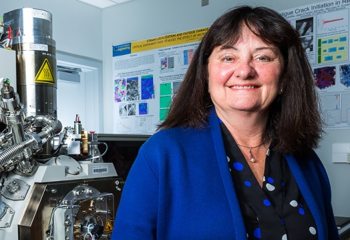
UCSB Alcoa Professor of Materials Tresa Pollock
Jan 03, 2018
The Minerals, Metals & Materials Society recognizes the UCSB materials professor and recent department chair for career-long leadership and contributions.
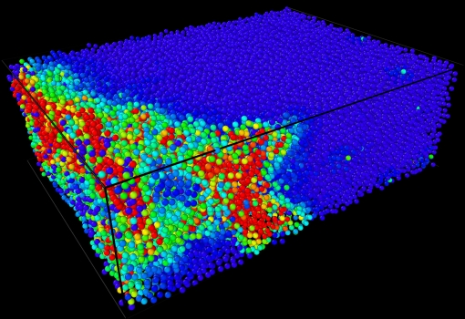
In this snapshot showing a reconstruction of a compression experiment, the red particles indicate hotspots, where atoms are rearranging as a prelude to failure.
Image compliments of Daniel Gianola, Daeyeon Lee, Jyo Lyn Hor, Daniel Strickland
Dec 13, 2017
Ordered, crystalline materials fail predictably. A collaborative group has identified a mechanism for predicting failure in disordered materials, too.
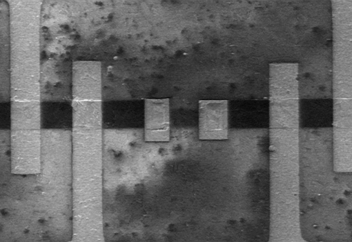
Scanning electron micrscope image showing two graphene connectors (center) and four other metal connectors.
Dec 11, 2017
Professor Kaustav Banerjee's lab pursues solutions to limitations of copper interconnects on chips.
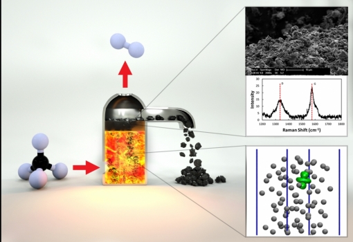
Fig. 1. Hydrogen production using a Ni-Bi molten catalyst
Photo Credit: Brian Long
Nov 21, 2017
UCSB researchers develop a potentially low-cost, low-emissions technology that can convert methane without forming carbon dioxide
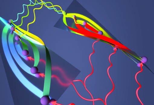
This artist’s rendition features Berry curvature represented by the twisting ribbons at the top.
Photo Credit: Brian Long
Nov 21, 2017
Physicists open the door to the first direct measurement of Berry curvature in solid matter
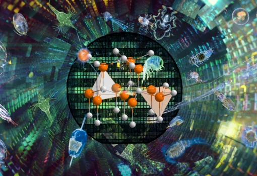
An arrtist's representation depicting a composite of marine materials
Nov 19, 2017
Researchers receive a $3.4 million grant from the NSF’s Office of Advanced Cyberinfrastructure to improve scientific image processing
- ‹ previous
- 17 of 22
- next ›