
For the past four-plus decades, the vast majority of semiconductors used in LEDs, optical communication, and light detection have been “III-V” materials, so called because they are compounds made by combining elements from groups III and V in the periodic table.
Kunal Mukherjee, an assistant professor in the Materials Department in the UC Santa Barbara College of Engineering, works extensively with III-V materials, but as a materials scientist, he is also interested in exploring new systems and developing new approaches to using familiar systems. He recently received a five-year, approximately $593,000 National Science Foundation CAREER Award to study IV-VI semiconductor materials, which are made of elements from those groups in the periodic table.
IV-VI materials predate III-V materials. Their properties were discovered around the 1870s, but they have been largely abandoned in electronics, because they are inherently soft and slow and can be easily damaged under the stresses of manufacturing.
IV-VI materials may have value, though, in addressing an inherent limitation of III-V materials. All crystalline materials have defects in their atomic structure, and provided the crystals are grown carefully, the defects in III-V materials are not problematic in most electronic applications; however, when III-V materials are used to make cost-effective devices that emit or receive light in the infrared spectrum, defects degrade performance. IV-VI materials, on the other hand, might be immune to some of the impacts of defects and loss when operating in the infrared.
“When you make devices to emit and detect at these [infrared] wavelengths, you have to grow them very, very carefully; otherwise, you can have whole rows of atoms that are not in the right place,” Mukherjee says. “A defect of this kind grows over time in the device as you’re running it, causing it to malfunction. We’ve seen how bad defects can be in III-V infrared lasers, so our long-term thinking was, can we find a material that has the intrinsic properties of a III-V material but is not as sensitive to defects?
The team hypothesizes that a unique mixture of metallic, covalent, and ionic bonding of atoms in a IV-VI material is what lends immunity to defects. “To address one part of the proposal, we want to try to verify this. We want to prove scientifically that there is immunity in the IV-VI, and then uncover the mechanism that confers the immunity,” Mukherjee says.
The researchers also want to know if III-V materials can be combined with IV-VI materials to create a kind of “best of both worlds” material that is structurally stiff, like III-V materials, but also immune to crystal defects in the infrared. Their initial attempts have involved using molecular beam epitaxy (MBE) to create a substrate of III-V materials, and then to grow IV-VI materials on top of them.
“The nature of the bonds between atoms in a material determines the properties of that material,” the team writes in the proposal. They want to see how the IV-VI material bonds atomically to the III-V and whether that changes the property of the semiconductor. Their challenge lies in the fact that the crystal structures for the III-V and the IV-VI are similar but different.
The team spent the past year learning how to overcome the difficult challenge of getting the IV-VI material to sit on top of the III-V substrate. “The interface is a new environment for the atoms, so they don’t know what’s going on,” Mukherjee says. “You have to coax the first layer of IV-VI atoms down onto the III-V substrate.”
Because the substrate is unfamiliar to the IV-VI atoms that are condensing onto it in the MBE chamber, sometimes the atoms land incorrectly. To overcome that, Mukherjee explains, “We gave the atoms time and a lot of second chances to correct the errors.”
They did that by making the substrate very hot. Mukherjee explains: “If an atom went down incorrectly, the heat gave it enough energy to pop back out and rearrange itself in a correct position. The substrate was not so hot, though, that it caused atoms that settled correctly to re-evaporate. Once the atoms were in place, the substrate was allowed to cool, and from that point, it was easy to grow more layers of IV-VI to achieve the desired thickness. Growing the top layer of III-V materials will likely involve overcoming similar challenges.”
Now that the team has reached this point, they can pursue the other challenges in the proposal. One of those is to use electron microscopy to understand why IV-VI have immunity to defects.
“We have a wonderful electron microscopy facility in our department, and we can actually locate an individual defect and then observe how that defect is sucking up all the charge in the material,” Mukherjee explains. “We’ll then change some of the properties of the material and the interface to see how that influences the defect.”
The team has deep expertise in III-V materials and is simultaneously growing them to provide a benchmark to use in comparing how IV-VI materials behave differently.
Another goal of the research is to attempt to create the materials in some exotic phases, such as topologically ordered states, which are of interest to those working in the new NSF-funded UC Santa Barbara Quantum Foundry.
Researchers have three chances to apply for an NSF Career Award; this was Mukherjee’s first try. “It’s such a relief to get the award,” he says. “The thing I like about it is that everything we submitted was homegrown by my students Brian Haidet and Eamonn Hughes in the past year to year and a half. It’s validation that it sometimes pays to take risks. I was trained in III-V materials and did all the III-V things, but we decided to go out on a limb to look at some more exotic systems that we can grow. The reviewers liked that we are a III-V group and can therefore more objectively evaluate the IV-VI system. To have a panel of exterior reviewers say it’s a risk worth taking is rewarding.”
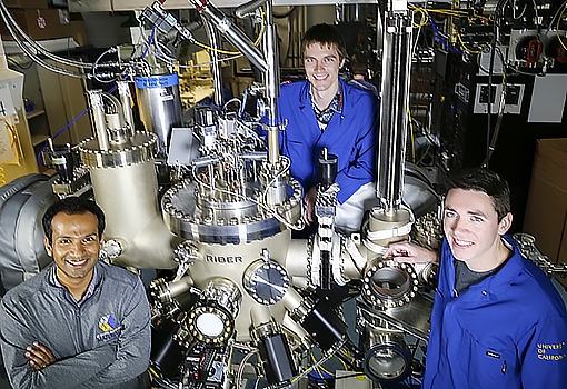
Kunal Mukherjee (lower left) with PhD students (from top) Brian Haidet and Eamonn Hughes in the MBE lab.