UCSB College of Engineering professors Steven DenBaars, Umesh Mishra, and James Speck began working with gallium nitride (commonly referred to as GaN) as a semiconductor in 1993, but at the time, funding for such research was largely unavailable because, as DenBaars recalls, “GaN was thought to be useless as a semiconductor.”
That was because GaN is a highly imperfect crystal. Typical LED semiconductors exhibit fewer than 100,000 defects (known as “dislocations”) in the crystal structure/cm2, and a silicon crystal may have as few 100 defects per square centimeter. But in 2000, no one had yet made a GaN substrate that had fewer than 1 billion defects/cm2. For that reason, when GaN is layered with other materials, those defects propagate in the crystal lattices, impeding performance of the semiconductor and electronic devices based on it. DenBaars, Mishra, and Speck spent years understanding how defects came into GaN crystals and how to address them and compensate for them in GaN–based semiconductors.
They also discovered that defects aren’t as much of a problem for GaN as they are for other semiconductor materials. “Generally, defects are bad for semiconductors, and they’re definitely bad for GaN, but it’s much more tolerant than other semiconductor, and we’re still trying to figure out why,” Speck said in 2017. “It’s like a diamond with millions of defects. That was the main reason people thought it wouldn’t work.”
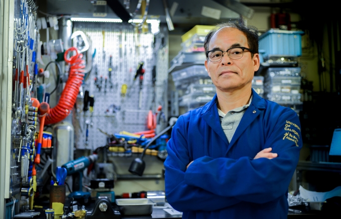
LEDs were the first technology to benefit from GaN. Early LEDs suffered from poor brightness and were limited in terms of color range and quality. Famously, in 1993 Shuji Nakamura, then a researcher at Nichia Chemical in Japan, and two colleagues at Nagoya University, used a GaN-based semiconductor to invent the blue LED, which enabled the white LED, which in turn revolutionized the lighting industry.
Understanding the promise of GaN-based electronics after Nakamura’s success using GaN with indium, DenBaars, Mishra, and Speck — who had been using GaN with arsenide — redoubled their efforts on GaN lighting, launching a series of systematic studies to understand its crystal growth and determine why Nakamura’s methods had succeeded. Nakamura came to UCSB in 2000 after DenBaars hand-delivered UCSBs offer to him in Japan, and since then, indium gallium nitride (InGaN) has been at the center of many important advances in solid-state lighting, laser diodes and power devices.
The GaN layer for early GaN semiconductors was grown on a sapphire substrate, but sapphire, like most substrates, is not conductive, and, DenBaars, explained, “Sapphire has a different atomic spacing in the crystal lattice than GaN, so there was a lattice mismatch.
“But GaN grown on GaN can have as few as 100 to 1000 defects per cm2 in the crystal,” DenBaars explained. Fewer dislocations mean much greater efficiency, so much so that a single GaN-and-GaN chip could replace ten GaN-on-sapphire chips.
The qualities of GaN crystals can be controlled to some extent by the process used to grow them, and in the late 1990s, Speck began studying how to grow the crystals using molecular beam epitaxy (MBE), a process in which the materials that form the GaN semiconductor are deposited manually onto a substrate. In 1994 DenBaars developed the process for growing GaN crystals using metal organic chemical vapor deposition (MOCVD), in which the material layers are created through highly controlled chemical reactions among gasses released into a chamber. Both MBE and MOCVD are used today, depending on the application.
The researchers would like to have started by growing grown GaN on a GaN substrate, but at the time, but in the early days of MBE and MOCVD, growth rates were not fast enough to provide bulk GaN material. “We could make GaN-on-GaN semiconductors only after someone figured out how to grow large-area bulk GaN,” DenBaars said. A breakthrough occurred in 2000, when Mitsubishi Chemicals developed a proprietary technique for producing bulk GaN crystals in bulk.
Since then, GaN on GaN has become an SSLEEC signature “Everyone else was using GaN on a sapphire substrate,” says Nakamura. “Using GaN on GaN lets us develop new devices that others can’t make.”
The GaN-on-GaN semiconductor was the key to developing brighter LEDs and creating the first high-efficiency LEDs in 2005, and to continued increases in efficiency ever since. A 40-percent-efficient green LED was produced in 2014. That rose to 50-percent efficiency in 2015 and to 60-percent in 2016. The most efficient blue LED now is now 84-percent efficient.
Many of the center’s ensuing successes have resulted from identifying other materials to combine with GaN to create the most-effective semiconductors, and understanding and addressing GaN’s idiosyncrasies and how they affect performance. “We’ve been pursuing improvements in efficiency through improvements in the material science and the process of generating the crystals,” DenBaars said. “We have probably one hundred patents in that area alone.”
“Fabrication techniques for GaN provide the base materials technology behind all the other applications,” added DenBaars, who likens GaN devices to a multi-layer cake: “You can layer it to be a light emitter, as a light bulb, or make it strong enough to emit laser radiation, or, in the case of Umesh Mishra, you can make an electronic cake that acts as a transistor and can emit radio-frequency waves. You can also layer the cake to receive light as a solar cell.”
The once “unusable” semiconductor has become a defining point of distinction.

Professor Shuji Nakamura
