
UC Santa Barbara Materials and ECE professor Chris Palmstrøm, who joined the UCSB faculty in 2007, was recently named a 2023 Fellow of the American Association for Advancement of Science (AAAS) in recognition of his contributions to fundamental materials science. We thought it would be interesting to take a deeper look at what earned him that recognition.
Tresa Pollock, interim dean of the UCSB College of Engineering, summarized Palmstrøm’s achievements, saying, “His indispensable expertise in using molecular beam epitaxy to control the growth and the interface structure and chemistry of dissimilar materials has led to the creation of many novel materials having new and useful properties. It is wonderful to see Chris be recognized for contributions that are important because they are truly impactful.”
Palmstrøm has spent decades creating new materials having novel properties, sometimes with an application in mind from the start, sometimes with the understanding that an appropriate application might come along only later. Either way, his research has generated important new knowledge that continues to inform pathways to future discoveries. He creates materials using a variety of methods, including the previously mentioned molecular beam epitaxy (MBE) as well as chemical beam epitaxy (CBE). The former is a method for using elemental sources to grow thin films atom-by-atom on a single crystal substrate in an ultra-high vacuum. CBE is a similar process, but in addition to elemental sources, molecular precursor compounds and gaseous sources are also used. Palmstrøm’s group is interested in the materials at the atomic level. “We want to understand how to put the atoms in the right place to control properties and create novel materials and structures,” he says
In an ultra-high vacuum environment, the surfaces remain clean, and one can utilize surface-science tools, most of which cannot be used at atmospheric pressure, to probe the structural, chemical, and electronic properties at the atomic scale during different stages of sample growth to gain detailed understanding of growth and interface formation. Palmstrøm has even developed an ultra-high-vacuum suitcase in which samples can be transferred without being exposed to air. In that way, they can be delivered to collaborators and to synchrotron facilities at the Advanced Light Source at Lawrence Berkeley Laboratory and SLAC at Stanford for further advanced characterization of electronic structure.
Conventional top-down processing involves etching structures onto a material after it has been grown, but Palmstrøm also uses bottom-up processing, in which the pattern of the structure is determined before the material is grown. This is achieved by growing a material only in selected areas. “To do this, I can deposit a dielectric material, such as glass, on a semiconductor surface and etch a pattern, such as a hole pattern, through the glass,” he says. “The semiconductor doesn’t like to grow on glass, and so, under selective-area growth conditions, it occurs only where the glass is missing.”
The value of selective-area bottom-up processing is that it allows fabrication to occur without the damage that is introduced by top-down etching, Palmstrøm notes. “This is especially important for nanostructures, and while MBE can be used, CBE is particularly good for achieving selective-area growth of compound semiconductors.”
Much of Palmstrøm’s work has required him to combine dissimilar materials. “For example,” he says, “we’ve grown single-crystal metallic compounds on top of a semiconductor, which gives us ideal interfaces between the two. We’ve also grown different types of metallic compounds this way, including magnetic materials, superconductors, and topological materials.”
Palmstrøm has been investigating magnetic and topological materials, in particular, magnetic materials, known as half metals, that behave as a metal for electrons having one spin and as an insulator for those having the opposite spin. These quantum materials are the subject of widespread current research, as they may be applicable for spintronics, and for building a topological quantum computer.
Palmstrøm becomes involved in projects in various ways. Once, he was simply curious about a new class of materials that might be used to address reliability issues in semiconductor devices. The work began, he says, with “looking at the crystal structures of different compounds and phase diagrams to come up with the ideas.” That motivated research that would lead him to investigate rare-earth monopnictides and transition-metal group-III compounds to develop more reliable contacts for III-V compound semiconductor devices. Incorporating these single-crystal rare-earth monopnictide nanoclusters embedded in III-V semiconductors has resulted also in improved performance of solar cells, thermoelectrics, and THz devices.
A different entryway to a project occurred years ago, when Palmstrøm was approached by a theorist who was interested in having a shape-memory material — one that remembers its shape and will return to it when heated (used for deploying antennas in space, dental braces, stents, and many other applications). He wanted such a material in the form of a single-crystal thin film that could be used to develop miniature mechanical actuators. Some of the materials that Palmstrøm helped to develop were magnetic and had great potential for spintronic applications, and although actual devices were not fabricated, he was able to demonstrate the effect in a free-standing single-crystal thin film.
Palmstrøm’s lab became quite involved in investigating the materials that Microsoft used to try to make the fundamental qubit device needed for its topological quantum computer. He also worked with UCSB physics professor John Martinis on materials issues related to improving the performance of a superconducting qubit before Martinis became chief scientist on Google’s effort to build a quantum computer. Google extended those results to develop an array of superconducting qubits in its Goleta lab, where it used its Sycamore chip to demonstrate “quantum supremacy” in 2019.
Palmstrøm says that he relishes being involved with pushing and testing new ideas. “You can have an idea and say, ‘Let’s try it; there’s no guarantee, you don’t know, and you can make mistakes,” he says, “but you have to be willing to stick your neck out and see what happens.”
“There are people who do absolute fundamentals but can’t make a device out of that work,” he notes. “In our group we make things such that, if you were to think of the right device, we could make the stuff for you to try to fabricate it. A lot of what we do is to follow our hunches, but we don’t always have the whole product in mind, the ultimate application. In that way, though, we gain a lot of knowledge that will be useful for the future.”
That occurred for Palmstrøm in the area of spintronics, in which the spin of the electron, and not just its charge, is critical to operating a device. “The MRAM [magnetic random access memory] and the read head on the hard disk of your computer are metallic spintronic devices,” he says. “Going beyond spintronic devices, the idea emerged that the spin of the electron, rather than its charge, could be utilized in semiconductor spintronic devices. That would, in principle, reduce power consumption dramatically. The goal became to put spins from a ferromagnet into a semiconductor.
“The challenge, which we succeeded in overcoming, was not only to inject the spins, but also to detect them and manipulate them in the semiconductor,” he continues. “The one thing we weren’t working on was a “real” device. We made all the pieces for a device, and even though the theorists had speculated about possible devices, in the end, no realistic novel devices were proposed. The killer application – the real thing to apply them to — was missing, but we are still optimistic that this research will have future applications.” As it turns out, Palmstrøm is now applying a lot of what he learned from those studies to superconductor-semiconductor structures that may lead to smaller and improved superconducting qubit devices for quantum computing.
“In the end, something often comes out of research that is useful that you hadn’t thought about,” he says. “The transistor was invented just to replace vacuum tubes, because their filaments burned out too easily, making them unreliable. But the transistor led to the invention of integrated circuits, which was a serendipitous result that has resulted in dramatic improvements in energy efficiency and the revolutionary semiconductor technology that we all rely on. I hope that fundamental research continues to be supported, as unexpected outcomes will happen that could solve major challenges and lead to new technologies.”
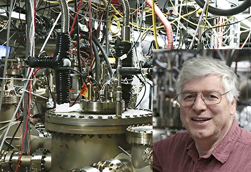
Chris Palmstrøm and the lab he built to create novel materials. Photograph by Lilli McKinney