
Several centers and institutes at UCSB serve as complementary, often-overlapping points of convergence for faculty, graduate students, and professional and postdoctoral researchers who share an interest in discovering faster, more-efficient, and cheaper ways of creating, moving, and using energy, and in identifying new ways to conserve it. Among them are the Institute for Energy Efficiency (IEE), AIM Photonics (within IEE); the joint UCSB-UCLA California NanoSystems Institute (CNSI), and the Solid State Lighting and Energy Electronics Center (SSLEEC).
Through those centers and institutes, researchers — including many world leaders in their fields — collaborate at the level of materials, devices, and systems to uncover the science and develop the solutions to produce low-cost, energy-efficient electronics.
IEE, AIM Photonics, CNSI, and SSLEEC also have strong records of moving research findings from the lab into the marketplace, where they have the greatest impact.
“The environment at UCSB is terrific for someone from industry who wants to come in and get a lot of work done really fast with top-caliber people,” said Ray Beausoleil, who leads the Large-Scale Integrated Photonic research group at Hewlett Packard Labs, which has partnered with UCSB researchers.
CNSI is directed by professor of chemical engineering, world-renowned polymer expert, and member of the United Kingdom’s Royal Society Craig Hawker and includes nearly forty affiliated faculty from UCSB engineering and the sciences. CNSI collaborators work in multiple areas of nanoscience, including energy efficiency. The Materials Department in the College of Engineering is particularly well represented in this area, where nanoscale work is aimed at developing new materials — and devices that incorporate them — to boost energy production, efficiency, and storage.
At the Bren School of Environmental Science & Management, researchers at the UC Center for Environmental Impacts of Nanotechnology have done groundbreaking work in determining the fate and transport of engineered nanomaterials on land and in freshwater and saltwater environments, in high-throughput testing of new nanomaterials based on experimental analysis of the effects of specific classes of ENPs on plant and animal life, and in leveraging nanoparticles’ unique characteristics in mitigating pollution.
The Institute for Energy Efficiency, numbers nearly eighty UCSB faculty among its affiliates, including Chancellor Henry T. Yang and Director John Bowers (electrical and computer engineering). The mission of the IEE, which is expected to be housed in its new building, Henley Hall, by fall 2020, is to realize major gains in energy efficiency and production in the following six areas, while advancing worldwide standards of living.
• Lighting: Long-term research is done to increase LED efficiency, an area of considerable overlap with the SSLEEC, where a team of faculty, including co-director Shuji Nakamura, who won a Nobel Prize for inventing the blue LED, work on a variety of projects based on the semiconductor gallium nitride.
• Energy Production & Storage: Research is pursued on leading-edge technologies include Professor Emeritus Alan Heeger’s work on flexible, cheap organic photovoltaic cells, themselves an extension of the conducting polymers he discovered and for which he won a Nobel Prize. Other faculty members, such as Gui Bazan, materials and chemistry professor and director of the Center for Polymers and Organic Solids at UCSB, continue to refine the technology. Additional topics include a new generation of lithium ion batteries, and batteries inspired by biology.
• Sustainability: The focus here is on integrating new technologies into the marketplace, while also understanding the social, environmental, and resource impact of those technologies. Life-cycle assessment tools are used to understand supply loops and to quantify the full range of impacts of products and services.
• Electronics & Photonics: The goal is to develop new wireless and optical communications technologies for interconnects that are 100 times more efficient. Replacing the electronic components that connect devices with photonic components could cut energy use by 20 to 75 percent.
• Computing: Data centers currenly consume some 1.5 percent of global energy, and the volume of data is increasing exponentially. Meanwhile, gains in computing-efficiency have slowed to a crawl. IEE researchers, including computer science professor Rich Wolski, inaugural holder of the Duval Family Presidential Chair in Energy Efficiency, are working to address the looming efficiency gap by reducing the energy use associated with cooling loads, inefficient server use, and wasteful computer processes.
• Buildings & Design: Buildings consume 72 percent of electricity in the United States and 40 percent of all energy produced in the U.S. IEE researchers like Igor Mezić are developing smart-building energy-management systems (see article on page 21) to accelerate the transition to zero-net-energy buildings.
Within IEE is AIM Photonics, the West Coast hub for President Barack Obama’s American Institute for Manufacturing Integrated Photonics (AIM Photonics). Directed by professor of electrical and computer engineering and AIM Photonics deputy chief executive officer, John Bowers, the center was created to develop an end-to-end integrated photonics manufacturing system in the U.S.
“We are working to develop science technologies that can save more energy than alternative energy sources can deliver,” says Bowers, a world leader in the field who in 2017 received the Photonics Award, the highest honor given by the Institute of Electrical and Electronics Engineers (IEEE).
Demand for high-performance silica photonics wafers is doubling every year. The wafers integrate multiple functions onto a single wafer, making it possible to overcome a fundamental incompatibility between the photons that carry data on fiber-optic networks and the electrons that carry data in computers. Large tech entities like Google want millions of units per year, but supply is currently insufficient to meet such demand.
AIM Photonics is meant to transform what Bowers described in 2017 as a “cottage industry” of small, independent manufacturers that produce individual pieces on ceramics into a nationwide industry that can produce integrated photonics wafers at enormous scale while driving the technology forward to give American manufacturing a key advantage in this important emerging area of technology.
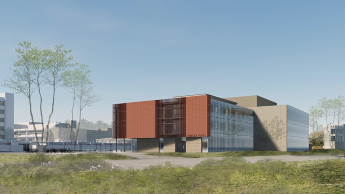
An architectural rendering of Henley Hall. The new home of the Institute for Energy Efficiency is expected to open in fall 2020.