
Wireless communications equipment, fiber-optics, light-emitting diodes, solar cells — we normally don’t give a second thought to these ubiquitous, often-undercover elements of modern life, but they empower technologies behind cell phones, communication satellites, laptop computers and data centers, and are the focal point for the booming fields of optoelectronics and solid-state lighting.
The shared elements running through all these advances are semiconductors, materials that have been coupled, layered, and otherwise engineered to move electrical current with previously unmatched efficiency, giving rise to the digital age. During their careers, two UC Santa Barbara College of Engineering professors (now emeritus) were responsible for breakthroughs that enabled these important technologies. Electrical and computer engineering professor Herbert Kroemer, who won the 2000 Nobel Prize in Physics, and UCSB materials professor Art Gossard, who received the National Medal of Technology and Innovation in 2016, worked independently and together for years to change the world in substantive ways.
“Herbert Kroemer likes to say that ‘all of the interesting physics is at the interface,’” recalled UCSB College of Engineering Dean Rod Alferness.
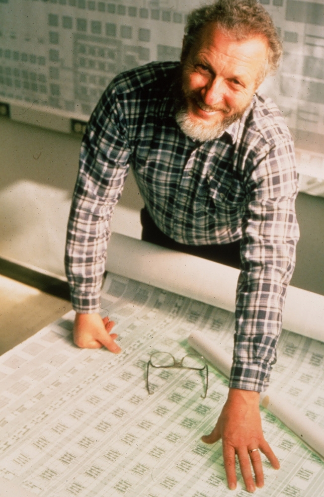 Herbert Kroemer
The interface he’s referring to is the “heterojunction,” where two layers of different crystalline semiconductor materials meet, each having a different band gap. Band gap allows for the control of the flow of current carried by negatively charged electrons and positively charged holes, from an energy generator to a collector, or device, that uses the electricity. At the interface of correctly partnered materials, it is possible to generate or modulate light, amplify signals, communicate with other devices on a network, and carry out a range of interesting functionalities associated with such heterostructured semiconductors.
HETEROSTRUCTURES AHEAD
In much the same way that transistors solved the design challenges inherent to vacuum tubes — bulky, fragile, short-lived devices that required a lot of power — the idea of heterostructured semiconductors originated in response to what Kroemer identified as a problem of mid-20th-century electronic technologies: they were slow, because they relied on conventional junction transistors, a type of semiconductor.
Working on transistors in the 1950s, when they were very new, Kroemer was already thinking about how to improve them — in particular, he recalled, he wanted to understand “how to make them fast.”
Kroemer was in his twenties. He had just received his PhD in theoretical physics from the University of Göttingen and was employed as the “house theorist” in the telecommunications laboratory at the German Postal Service. It occurred to him that a semiconductor that had a “graded composition” — one that transitioned smoothly between one material having certain electronic properties and another material having different but complementary properties — could push the charge-carrying electrons and holes from an emitter to a collector in the way required to operate the device. He referred to this notion in a paper published in 1954, but the idea was ahead of its time, and no technology was available to prove the concept.
“Part of the power of Herb Kroemer’s idea was that he was proposing those kinds of structures even before anyone knew how you could make them,” Alferness said. “But he understood the physics.”
Kroemer would return to his concept of heterojunctions in 1957, in a paper he wrote on improved transistor performance while a researcher at RCA’s David Sarnoff Research Center at Princeton University.
“I simply asked what the consequences would be if you were to change this energy throughout the structure — not from the perspective of a particular transistor but just from the perspective of the physics.”
That line of questioning would lead to the concept of the quasi-electric field — a characteristic of semiconductors having varying band gaps — which offers more control over the direction and movement of electrons and holes. It was a powerful concept, Kroemer said, but again, there was no way to prove it at the time.
Six years later, as a scientist at Varian Associates in Palo Alto, California, Kroemer was listening to a colleague’s talk about newly invented semiconductor lasers, which, Kroemer said, were exciting but at the time, little more than a “laboratory curiosity,” because they could emit light only in pulses and at very low temperatures. The lecturer himself described a continuous-operation room-temperature semiconductor laser as “fundamentally impossible.” Kroemer disagreed; in fact, he already had a solution mapped out for concentrating the charge carriers that needed to meet in order to produce continuous laser light.
"I had always said we needed someone like Art Gossard. I was a great admirer of his work, and he was known to be a fabulous collaborator."
“The challenge with the laser is that you need very large numbers of electrons and holes,” Kroemer explained. When an electron meets a hole, the electron transitions to a lower-energy state, releasing energy as light. The problem in homogenous semiconductors, he added, was that the charge carriers flow through in opposite directions as quickly as they are supplied. But with a double heterostructure consisting of two low-conductivity, large-band-gap semiconductor layers sandwiching a highly conductive, lower-band-gap material, with other elements added to keep the carriers from exiting the material on either side, enough electrons and holes could be brought together in the middle layer to emit coherent, or steady, light. This notion of a double heterostructure would later be refined to create the “quantum well.”
But the success of the compound semiconductor depended enormously on the transition between the different materials — the heterojunction. The crystal lattices into which the semiconductor materials were organized had to match, or align, in a way that would allow the mobile carriers to pass easily from one material into the next. The technology to create such perfect alignments did not exist yet, but research was gaining momentum as scientists everywhere sought out ideal combinations of materials and methods for fabricating those structures.
THE PERFECT MATCH: PIONEERING THE SUPER-THIN
From the late 1960s into the ’70s, Bell Labs was a hotbed of research and development. Lasers and optical fibers had been developed there as the first technologies to use light to transmit information. Both were significant developments in the field of optics, but it would not be possible to make a high-quality double-heterostructure laser until the super-thin layers of semiconductor material itself could be fabricated with better precision and purity.
At around the same time that Kroemer joined the UCSB engineering faculty in 1976, Art Gossard was a Bell Labs scientist who was becoming known for his mastery of an emerging technique for creating new materials, called molecular beam epitaxy (MBE). Developed in the late 1960s by Bell Labs scientists Alfred Y. Cho and John R. Arthur, Jr., MBE is a method of “growing” a film of one material on top of another by depositing each layer, atom by atom, in an ordered fashion.
“Being able to put one crystal layer onto another gave you what you needed to make improved transistors and lasers,” said Gossard, who had come to Bell Labs just after receiving his PhD in physics from UC Berkeley in 1960. A specialist in solid-state physics, his interests led him to investigate such phenomena as nuclear magnetic resonance (NMR) in ferromagnets, and to apply NMR spectroscopy and other advanced techniques to make measurements of new materials.
“I thought the materials themselves were actually more interesting and important than making measurements on them,” he said, so he began focusing on MBE, and Bell Labs responded by pairing him with “genius machinist/super-technician” Bill Wiegmann to work with the earliest versions of MBE machines. “You couldn’t buy an MBE system back then,” said Gossard. The equipment had to be made in-house and required special attention.
Soon, Gossard and his team were turning out new materials and measuring interesting electron behaviors. Other scientists were turning to them with their ideas for materials and benefiting from Gossard’s solid-state physics expertise and Wiegmann’s technical acumen. They could fabricate increasingly sophisticated materials with, for instance, quantum wells having graded sides to control the behavior and movement of charge carriers. That process — adding strategically placed atoms to a material to provide electrons precisely where they are needed — is referred to as “doping.”
“We worked more on tailoring the structure than on the chemical composition,” Gossard explained. “You could build a quantum well of any shape, but purity and smoothness of the material were of utmost importance.”
Back in California, Kroemer was realizing the potential for using MBE to fabricate semiconductors from different materials having highly crystalline qualities, provided the two materials had the same lattice constants, or dimensions of unit cells so that they could align.
“I decided that molecular beam epitaxy is something that even a theorist can understand,” Kroemer quipped. His job included helping to amplify and steer research efforts at UCSB’s solid-state laboratory, which was part of the university’s emerging College of Engineering.
Instead of jumping into what had already become the highly competitive field of silicon semiconductor technology, Kroemer had convinced Ed Stear, then-chair of the Electrical and Computer Engineering Department, to focus on compound semiconductors, which were already showing promise. As part of the effort, Kroemer had managed to acquire an MBE machine, only the second one to be sent to a university.
“He was able to buy one, which was amazing, because he was a theorist and not an experimentalist,” said Gossard, explaining that in the late 1970s and ’80s, MBE was still a relatively new technology. “But on the other hand, he was a very determined visionary, and he saw the opportunity.”
Gossard visited and spoke at UCSB in 1979 during the second-ever MBE conference in the United States. The gathering, organized by Kroemer, hosted the small but growing community of scientists and engineers interested in the technology and its applications.
Kroemer had his eye on the MBE expert.
“I had always said we needed someone like Art Gossard,” Kroemer recalled. “I was a great admirer of his work, and he was known to be a fabulous collaborator.”
The campus began to court Gossard as part of the concerted effort to build its compound-semiconductor activity. At first he resisted; he was happy at Bell, but then came the antitrust court decision in the ’80s that split the Bell system into smaller companies. Meanwhile, UCSB had managed to recruit another Bell Labs scientist, Pierre Petroff, who had been Gossard’s top collaborator at Bell. Thanks to circumstances he could not have foreseen, Gossard recalled, “UCSB was beginning to look more attractive.”
By the time he joined UCSB in 1987, along with trusted development engineer John English, materials research was ramping up. The Materials Department was established that year, and a steady stream of top faculty and researchers, many from Bell Labs, had been arriving. Among them were Vincent Jaccarino, who arrived at UCSB’s Department of Physics before Kroemer came to campus, and Jim Merz, whom Kroemer brought in. In fact, the Bell breakup proved to be an opportunity for Kroemer’s efforts to bring world-class engineers and scientists to the campus.
“Jim and I raided Bell Labs and brought in Larry Coldren, Evelyn Hu and John Bowers, in addition to Pierre Petroff,” Kroemer said. Not long after, Jim Allen was recruited to the Department of Physics upon Gossard’s recommendation.
“UCSB has always excelled at collaboration,” said Gossard. Kroemer would agree: he recalled that the opportunity to build a community around his science was a driving factor that brought him here.
A PAYOFF IN BREAKTHROUGHS
What started as something of a gamble paid off, as UCSB gained prominence in the field of compound semiconductors. Electronics and photonics research on campus has grown largely around theories and discoveries related to heterojunctions and the methods by which two different materials are fused to achieve specific attributes. The materials program has consistently been ranked first in the nation among such programs at public institutions.
Gossard would go on to co-discover the quantum-confined Stark effect — used to create fast, efficient fiber-optic light switches and quantum computation devices — and the fractional quantization of the Hall effect. The latter, which won the 2008 Nobel Prize for some who worked on it, is a new, unanticipated, ordered low-temperature quantum state found in sheets of electrons within strong magnetic fields. The innovations that led to that discovery also enabled electron “superhighways” in semiconductors, which are now the basis for high-performance transistor circuits in a range of technology, including today’s cell phones and satellite receivers.
"The gamble paid off, as UCSB gained prominence in the field of compound semiconductors."
Other recent breakthroughs by Gossard and his collaborators include improved thermoelectric materials that enable efficient generation of electricity directly from heat, improved broad-spectrum solar cells having record efficiencies, and quantum dot lasers. Grown directly on silicon, quantum dot lasers enable maximum communication and control within silicon integrated circuits. In 2016 Gossard received the National Medal of Technology and Innovation, the nation’s highest honor for technological achievement, given to recognize those who have made lasting contributions to America’s competitiveness and quality of life.
Kroemer earned his Nobel Prize in Physics for inventing semiconductor heterostructures. The technology continues to underlie cutting-edge research on campus, including discoveries that led to UCSB professor Alan Heerger’s winning the 2000 Nobel Prize in Chemistry for his discovery of conductive polymers, and materials professor Shuji Nakamura’s winning the 2014 Nobel Prize in Physics for creating the bright blue LED.
Kroemer and Gossard’s research has had a global footprint. Countless technologies that are part of our daily lives — from smartphones, computers, and lighting to advanced machines for telecommunications, data transmission, and sensing — are made possible by semiconductor heterostructures. At UCSB, this essential technology has inspired tech spinoff companies, numerous patents, and close partnerships with industry. The work also continues to inform research on campus, as scientists, engineers, and their students strive to increase their understanding of quantum physics so that they can develop the high-performance, energy-efficient materials that will enable future technologies and solve 21st-century challenges.
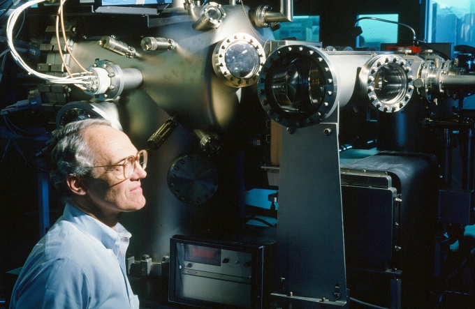
Art Gossard with a molecular beam epitaxy machine he helped create.