Research at UC Santa Barbara reveals how a phenomenon first discovered 100 years ago impacts state-of-the-art devices.
.

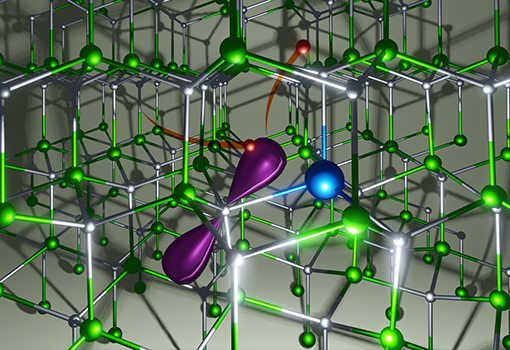
Concept illustration depicting the trap-assisted Auger-Meitner process at a calcium substitutional impurity (blue) in a gallium nitride crystal lattice (green and silver spheres). An incoming electron (red) gets trapped in a localized state (purple), and its energy is transferred to another electron. Illustration by Fangzhou Zhao.
Research at UC Santa Barbara reveals how a phenomenon first discovered 100 years ago impacts state-of-the-art devices.
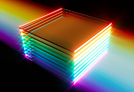
Artist's concept illustration depicting a stack of heterogenous materials similar those used in this project. Illustration by Brian Long
3D integration of monolithic and heterogeneous layers allows the Bowers lab to achieve an important milestone.
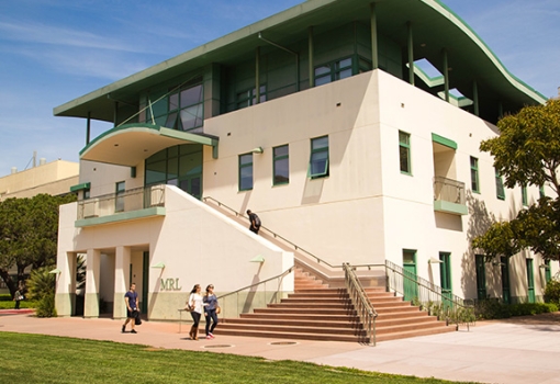
UC Santa Barbara’s Materials Research Laboratory (MRL) has received its seventh consecutive major grant from the National Science Foundation.
The Materials Research Laboratory received its seventh consecutive major grant from the National Science Foundation.
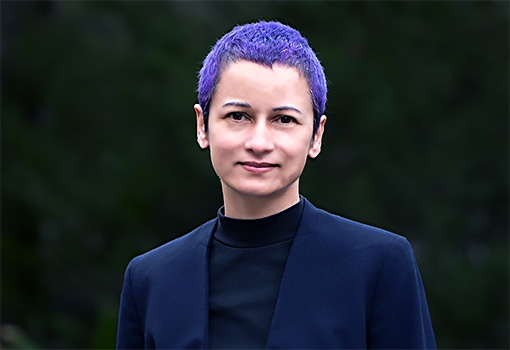
Computer science assistant professor Misha Sra. Photograph by Lilli McKinney
The UCSB computer science assistant professor is using AI to make all kinds of learning accessible.
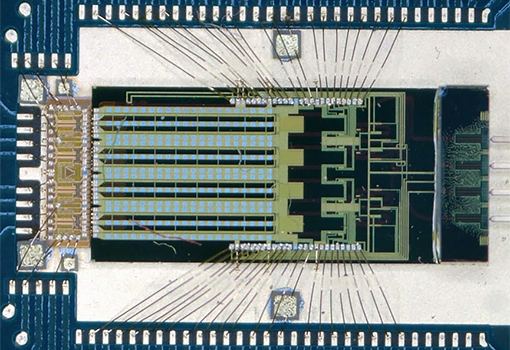
An image of the newly developed transmitter assembly. The small, brownish chip on the left is the electronic integrated circuit (EIC), and the larger, black-and-gold chip on the right is the photonic integrated circuit (PIC). The long structure on the left side of the PIC is the modulator, which converts the electrical signal into an optical one. Light gets coupled into and out of the chip through the fibers on the right side of the PIC. Everything is mounted on a printed circuit board (PCB), with gold wire bonds connecting the chips. Data flows from left to right, where the incoming electrical signal gets amplified by the EIC, converted to an optical signal by the PIC, and sent out via fiber to its destination.
Holistic co-design of photonics, electronics, and packaging enables faster, more-efficient data transfer.
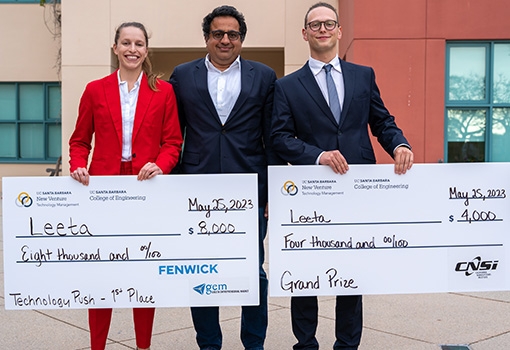
Leeta team members, Kira Wyckoff (left)) and Linus Kautzsch (far right), with their advisor Ram Seshadri
The team received $12,000 in prizes for their novel manufacturing process to produce high-demand battery materials.
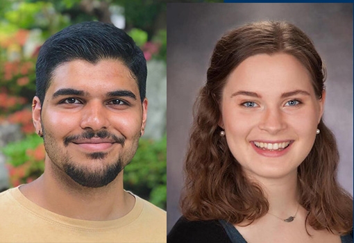
Materials PhD students Tanay Tak (left) and Bailey Rhodes, 2023 National Defense Science and Engineering Graduate Fellows
Pair of materials PhD students win prestigious fellowships from the Department of Defense.
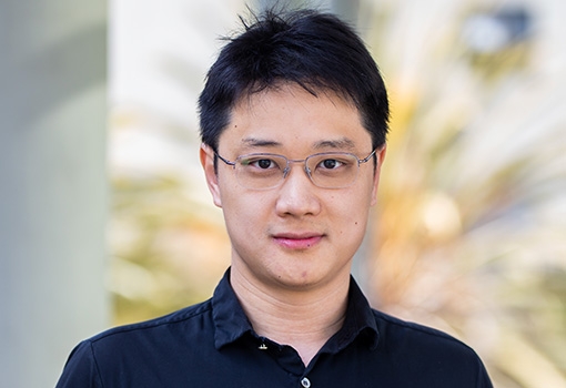
UCSB postdoctoral researcher Chen Shang
A UCSB postdoctoral scholar earns international recognition for his innovative research.

The 2023 New Venture Competition Finals will be on Thursday, May 25.
The six teams will compete for thousands of dollars in prize money during the NVC Finals on Thursday, May 25.
From left to right: Ambuj Singh, Christopher Kruegel, Joao Hespanha, Giovanni Vigna; Photo Credit: Matt Perko
UCSB will serve as the lead in a five-year, $20 million project to establish the Institute for Agent-based Cyber Threat Intelligence OperatioN (ACTION).
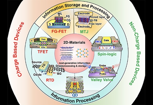
An array of charge-based and non-charge-based devices built with 2D materials may enable next-generation information processing and storage technologies. Four of the most promising devices — the spin-FET and the TFET (both for processing) as well as the FG-FET and the MTJ (both for storage) — are covered in the article. Illustration by Arnab Pal
New devices from Kaustav Banerjee’s lab show promise for next-generation information processing and storage.
Assistant Professor Johanthan Balkind.
He plans to use microarchitectural checkpointing to redesign processors to improve cloud-based computing.