
Every year, the demand for Internet bandwidth and performance grows by leaps and bounds, as more gadgets — particularly mobile devices — come online, more data-intensive applications appear, and all the devices networked in the emerging Internet of Things flood telecommunication highways with endless streams of information. In 2015 alone, demand for mobile bandwidth jumped by 74 percent, and the deluge of data shows no signs of stopping.
The infrastructure that makes our digital lives possible is straining to keep up with demand. Adding capacity to data centers and improving storage networks are two stop-gap approaches to coping with the growing river of data, but adding more machines requires more energy, both to operate the equipment and to keep servers cool so that data is protected.
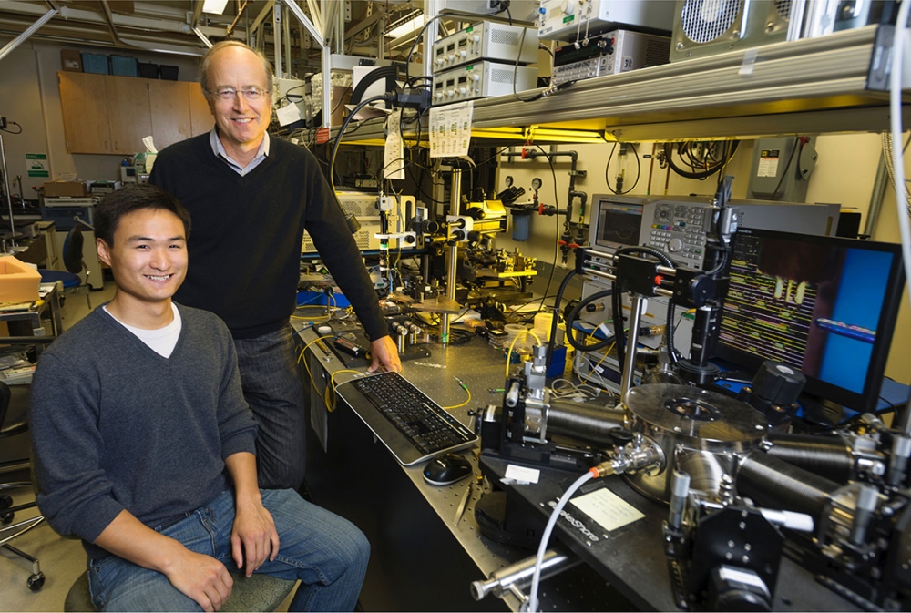
UC Santa Barbara professor of electrical and computer engineering John Bowers has had this critical digital-age challenge on his radar for a long time. A world-renowned authority on photonics and optoelectronics, both of which involve using light to move data with extreme speed and efficiency, he is working with fellow UCSB faculty and researchers to provide a scalable solution to the problem of data overload. It involves integrating silicon photonics more deeply into communications and data processing.
In 2013, the federal government put its weight behind an effort to increase energy efficiency and achieve high-performance data transmission while creating and retaining high-tech manufacturing jobs in the U.S. and accelerating research to address such challenges as rising energy needs, aging energy infrastructure, and the need for better materials. Following a competitive process, the American Institute for Manufacturing Integrated Photonics (AIM Photonics) was established in 2015 as a $500 million public-private initiative. UCSB was selected as the West Coast Hub, and Bowers, who is director of UCSB’s Institute for Energy Efficiency, was named West Coast director. He is now working with colleagues across the United States to develop silicon photonics — now in its infancy — into one of the nation’s leading tech industries.
“UCSB’s selection as the West Coast Hub for AIM Photonics provides a strong, direct indication of the high value and recognition of the scientific and engineering research breakthroughs that have resulted from our many faculty-student collaborations in this field,” said College of Engineering Dean Rod Alferness.
“Silicon photonics has the potential to revolutionize photonics and electronics by enabling low-cost, high-volume manufacturing of optical interconnects, with a path toward embedding high-capacity fiber optics on circuit boards and, eventually, on electronic chips,” said Bowers.
Photonics in communications is already present in the form of fiber-optic cables, which came into use in the late 1970s, when phone companies began to build and upgrade their infrastructure using the high-speed, low-loss technology. The national grid of fiber-optic cables proved invaluable during the rise of the internet.
“The internet would not be possible without this whole infrastructure of fiber cable carrying huge amounts of information, which it does extremely well,” said Alferness, who, in his previous career as chief scientist at Bell Labs, witnessed first-hand the enormous potential photonics had in terms of revolutionizing communications.
Currently, connecting electronics and photonics is costly and inefficient. Computing is done electronically, and to get on the fiber-optic highway, the electronic bits have to become optical — photonics and electronics must be brought together.
“Right now, that’s being done discretely,” Alferness said. “Separate modules do the optics and the electronics.” It works, he added, but the equalization takes a lot of energy and generates heat, which can drastically reduce the performance of the silicon chips. “We know that if we can get that electrical signal converted to an optical signal on the silicon chip, it can be not only cheaper, but also much more energy efficient. We win twice, because we will need less power to get the electronic signals off and less power to do the air-conditioning.”
Developing the technology is only the beginning. For photonic integrated circuit (PIC) and switch technology to flourish and have the imagined far-reaching impacts, an entire photonics manufacturing ecosystem, from lab to market, must be established. That means amplifying research, broadening the market, developing and implementing manufacturing logistics, and training a workforce. Creating that ecosystem is the responsibility of the nationwide network of AIM Photonics partners in industry, academia, and government.
Academic participants include the SUNY Polytechnic Institute — lead university in the endeavor — as well as MIT, the University of Rochester, the University of Arizona, Rochester Institute of Technology, Columbia University, UC Berkeley, UC Davis, and UCSB. Industry partners include Infinera, Cadence, Boeing, and Raytheon, while the U.S. Department of Defense, NASA, the Department of Energy, the National Science Foundation, and the states of New York, California, and Massachusetts are also involved.
Beyond Bowers, UCSB has tremendous prowess in research related to silicon photonics materials, including electrical and computer engineering, mechanical engineering, and energy efficiency. Three of the six UCSB Nobel Laureates were recognized for innovations related to optics: Herb Kroemer, inventor of the double heterostructure laser; Alan Heeger, inventor of conductive polymers; and Shuji Nakamura, inventor of the blue LED. The interdisciplinary environment at UCSB enables collaborations among some of the best researchers in the field.
A growing number of graduate students and postdoctoral researchers, encouraged by their mentors and supported by peers in UCSB’s top-notch engineering programs, play important roles in this research. These brilliant, highly motivated young people routinely join forces on collaborations that result in important innovations on the path to integrating photonics and electronics.
Undergraduates, too, are attracted by the combination of teamwork, the track record of success, and the desire to improve life through technology that infuses the UCSB College of Engineering. AIM Photonics’ educational outreach efforts include a research undergraduate apprenticeship at UCSB. First- and second-year engineering students, plus students from local community colleges, are invited to participate in an eight-week program, which provides them with technical and professional training in photonics. The apprentices participate in relevant research, receive guidance from the more senior members of research teams, and gain opportunities to meet and network while learning about the practical aspects of a career in photonics.
“The AIM apprentice program exposes students to leading research and gives them the opportunity to learn research skills, interact with professors and graduate students, and advance state-of-the art research,” Bowers said. “It is a great chance to see if a life of research, or at least graduate school, is of interest to them.”
Opportunities to collaborate with and work in the photonics industry are never far from students and researchers at UCSB. The campus’s Center for Science and engineering Partnerships, led by Ofi Aguirre, is responsible for developing, managing, and executing the education and workforce-development components for the AIM Photonics West Coast Hub. The UCSB Materials Research Lab has also played a role in recommending students whose interests lean toward photonics research, and providing resources for that research.
Many professors in the College of Engineering have strong backgrounds in industry and have licensed their inventions to existing companies, have created and run their own startups, and have relationships with companies that support their work.
All that multi-layered collaboration and partnership adds up to an environment in which academia and industry can easily network, trade ideas, share facilities, and innovate — all with the goal of designing and manufacturing PIC technology that increases data and telecom performance and energy efficiency for small and large enterprises alike.
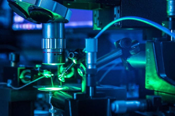
A silicon-circuit testing station in an AIM Photonics lab.