
A new age of 3D printing is here, even though the initial technology for what is also known as additive manufacturing arrived less than twenty years ago. UC Santa Barbara is stepping into the era thanks to a $1.15 million grant from the National Science Foundation (NSF) to purchase the most cutting-edge 3D printing technology available: a 3D rapid nanoprinting system based on two-photon photolithography. The equipment will enhance the capabilities of the already widely recognized UCSB Nanofabrication Facility, (aka the “Nanofab” or “Nanotech”).
“The unique capabilities of this system open the door to new approaches to nano- and micro-manufacturing of complex structures and devices that are no longer constrained by geometry nor confined to two-dimensional planes,” the authors write.
 By securing the grant, lead PI Galan Moody (left), UCSB professor of electrical and computer engineering, and four co-PIs — Marley Dewey (Bioengineering), Andrew Jayich (Physics), Sumita Pennathur (Mechanical Engineering), and Andrea Young (Physics) — are ensuring that UCSB can take a leadership role in pushing the boundaries of what the new technology can do. Says Moody: “There are just a few universities in the U.S. that have tools with these capabilities.”
The tools are needed, the proposal reads, “because we are at the limit of what can be achieved with existing nanofabrication tools, which have enabled wafer-scale fabrication of semiconductors, dielectrics, and metals with resolution down to approximately ten nanometers [nm], but only in a planar [essentially two-dimensional] geometry. Additional complex, time-consuming steps are required to create increasingly essential 3D microstructures.”
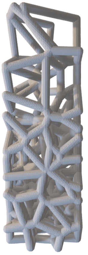
Advances in the past couple of years have brought 3D printing to the realm of the very small, supporting an array of applications by enabling on-chip 3D printing of microstructures, a capacity that will benefit researchers in many disciplines.
Moody provides an example to illustrate a limitation of the first 3D printing technology. “Normally,” he says, “you start with a semiconductor wafer [typically silicon] and use photolithography to yield a semiconductor with a pattern that has been transferred to it. If you look top down, it's just a 2D pattern. There is depth to it, but it's more like a thin film that’s maybe a few hundred nanometers thick, so you can’t raster-scan it in all three dimensions to make a nice 3D structure. Ten-nm-resolution lithography is available at off-campus commercial foundries, but none is capable of creating complex 3D structures with nanoscale resolution and high speed for high-throughput prototyping, which are required for next-generation devices. Being able to make structures in true three dimensions opens new capabilities.”
Five Researchers, Five Uses
The principal investigators’ research reflects the diverse focuses of potential users — and uses — of the new equipment.

Moody, an expert in integrated quantum photonics, will create new photonic chip designs for ultra-efficient entanglement distribution and networking (example above; photographs courtesy of Nanoscribe): Panel A: A top-down view shows seven tiny lines — wave guides — at the edge of a photonic chip. Light travels from the chip to another component, such as a fiber optic cable. The flaring bright spots (bottom) are 3D-printed lenses that prevent the light from diverging as it leaves each guide. Panel B: Direct-write printing on fiber of a triangular component that creates a smooth transition between the smaller-diameter light from the wave guide and the larger-diameter fiber optic cable (right). Panel C: A spherical “ball” lens about 30-40 microns wide and a wave guide (entering from bottom right) that was printed to it. Light enters, hits the sphere, and is then launched up. Smoothness is key, because jagged edges can trap or scatter light, resulting in loss.
Jayich will apply his expertise in trapped ion systems to microprint 3D ion traps for optical clocks. Some of what he needs for experiments is not available on campus, and off-campus commercial vendors — except those who sell the new 3D-printing tools — are unable to provide what he needs for rapid fabrication of prototypes. The new tool will enable rapid prototyping of 3D-printed ion-trap structures on campus.
Dewey has a newly established research program at UCSB combining biomaterials with extracellular vesicles for skeletal repair and disease treatment, including broader impacts in coral regeneration and repopulation. She plans to use the system to create patterned biomaterials, or scaffolds, like the one shown at left, which can be used for a variety of purposes.
Pennathur intends to 3D print micro-systems to analyze fluids, and also to make micro-fluidic channels on chips. Researchers in her lab engineer micro- and nanofluidic systems to study how fluids, ions, and biological molecules behave when confined to channels approaching nanometer scales — where surface chemistry, Debye layers, and geometry — rather than bulk fluid properties — govern transport. 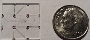 A central goal is translating the physics of such processes into functional devices, such as biosensors, passive flow-control systems, and implantable therapeutics that regulate themselves without external actuation. 3D printing enables rapid iteration on device architectures that would otherwise require weeks of cleanroom fabrication, accelerating the path from physical insight to working prototype. The photograph above shows a nanofluidic channel with integrated electrodes, with a dime for scale.
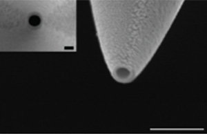
In Young’s research, he combines nano-fabrication and electronics to investigate the properties of electronic states in quantum materials. He can use the 3D-printed tool to create what he calls a nano-SQUID, or superconducting quantum interference device, and attach it to the tip of an atomic-force microscope to enhance its ability to characterize materials. The image below shows a nano-SQUID that Young would be able to print in-house.
All of the PIs will work closely with the Nanofab technical and operational director, Brian Thibeault, to coordinate system installation and qualification, as well as to implement training and the educational outreach activities described below.
Like Jayich, Moody would like to do in-house work that is currently either not being done or has to be sent to vendors for required engineering. “Using the new tool to do it ourselves has multiple benefits,” he says. “We do the work faster and for less cost, my students will get trained on the very best equipment, and we can share the in-house knowledge with the rest of the UCSB photonics community.”
Fueling the Future Workforce
Any new technology requires a workforce of people who can use it, especially in industry, and Moody sees educating students as a high priority. The proposal spoke convincingly about plans to train not only UCSB students on the equipment, but also local community-college students. That gives those students, many of whom are first-generation college students, access to good jobs without having to earn a PhD or, perhaps, depending on their circumstances, attend university at all. “They will learn to use the equipment if they go through one of our boot camps or participate in one of the many UCSB internship programs operated with the support and leadership of the Center for Science and Engineering Partnerships,” Moody says.
Those programs include the Central Coast Partnership for Regional Industry-focused Micro/Nanotechnology Education (CC-PRIME). Led by Santa Barbara City College and run through the California NanoSystems Institute (CNSI) at UCSB, CC-PRIME partners with local technology companies of all sizes and regional community colleges to train students in nanofabrication skills. It is part of a broad effort to build a regional educational pipeline to cultivate the micro/nanotechnology workforce.
Some students who participate in such programs might then opt to pursue a four-year degree or attend graduate school, but not all companies need someone with an advanced degree to run their fabrication processes. “If students have a certification saying, ‘I've gone through these boot camps,’ then they become valuable assets to companies,” Moody observes. “That might lead some students to think, Hey, I can do this. I've got the skills. Let me go get a job” now.
What Makes the New Tech New
While both the original and the new processes of 3D printing share a name, the earliest technology was actually more of a two-dimensional framework, Moody explains. “Three-dimensional objects could be created, but only by aggregating (the ‘additive’ part of “additive manufacturing,” as the first generation of 3D printing was also called) very thin layers of materials, which had length and width but no real depth.
Quantum networks, secure quantum communications, quantum sensors, and optical quantum computers and simulators require high-quality sources of entangled photon pairs, and much research is devoted to improving source quality, especially the pair-generation rate (PGR) which is the number of photon pairs extracted from the chip per second. The proposal explains that, Optical extraction efficiency from integrated chips to fiber is limited by the diameters of the various modes, which, typically, differ from each other by ten to fifty percent for quantum networking. To get around that discrepancy and “get the light into the fiber,” Moody says, “we bring the fiber right to the edge of the chip to capture it before it can diverge.”
The new system makes it possible to print a tiny polymer lens fewer than fifty micrometers wide onto the edge of a chip, enabling it to guide the optical mode. Fig. 3, Panel B shows an optical fiber and a small 3D-printed cone on the end of it that also acts as a lens to focus the light so that it goes into and propagates down the fiber rather than scattering as “loss,” a big problem in photonics.The lens can be printed either on the edge of a chip or on a fiber, as long as the light coming out of the chip is “matched to collect into the fiber,” Moody says.
“We try to arrange the components such that the light doesn’t “see” the fiber as a discontinuity. That allows the light beam coming out of the photonic chip to couple nicely into the fiber and keep going, resulting in very low loss,” Moody adds. “That's really hard to do, because there is often a mismatch between the shape of the optical beam in our small wave guide and how it looks in the much-larger fiber. To make the transition requires a smooth 3D structure without any jagged edges, which can trap or scatter the light, resulting in loss.
Smooth nanoscale 3D printing is essential for many structures and devices being made at UCSB. The new 3D printing technology can deliver it.

Co-PI Andrew Jayich will use the new technology to create ion traps like the one shown here, in which colors indicate independent electrodes to control trapped ions. Illustration by Brian Long.