Researchers will work toward improving efficiency in electric motors, quantum computing, and large language models with IEE support.
College of Engineering News

Bassam Bamieh, Mechanical Engineering Professor at UCSB
Oct 09, 2025
Bassam Bamieh seeks to model the dynamics of small disruptions that can trigger big failures in complex systems.

Bioengineering assistant professor Marley Dewey, a 2025 Hellman Family Faculty Fellows
Oct 06, 2025
Award supports work to outsmart bacteria and pioneer new therapies for implant-associated infections.

Artist's concept illustration showing a two-dimensional collection of interacting spins in a diamond lattice. Illustration by Brian Long
Oct 03, 2025
The road to realizing the promise of quantum applications has begun with a deep dive into the fundamental science of quantum phenomena to understand how they manifest — and how they might be made to manifest — in individual platforms.

Sep 26, 2025
A seaweed-derived gel that helps scientists understand how cells grow in their environment could be used for breast cancer research.

Sep 24, 2025
UCSB launches new facility with first-of-its-kind automated anaerobic chamber for studying unusual microbes.

Sep 23, 2025
The UCSB computer science professor will research quasi-polynomial time algorithms and their use in graph problems.

Sep 17, 2025
Undergraduate students from the Materials Research Laboratory’s internship programs presented the results of their summer research projects.

Sep 15, 2025
The UCSB mechanical engineering professor will study the dynamics behind mudslides, erosion, and other phenomena involving moving sediments.

Sep 11, 2025
The innovative tool, designed specifically for non-expert users, improves airway access and raises survival odds in critical medical emergencies.

UC Santa Barbara has entered into a long-term lease for a 105,000-square-foot-facility within Goleta’s tech corridor and adjacent to campus.
Sep 08, 2025
The facility will accelerate technology translation and national economic growth.

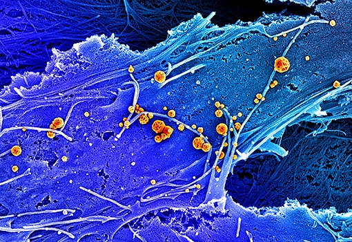
False-colored scanning electron microscopy image of human fibroblasts secreting (orange) matrix-bound nanovesicles. Illustration courtesy of Marley Dewey.
Sep 02, 2025
UCSB assistant professor of bioengineering will study extracellular vesicles that support tissue repair.
- ‹ previous
- 4 of 30
- next ›

